
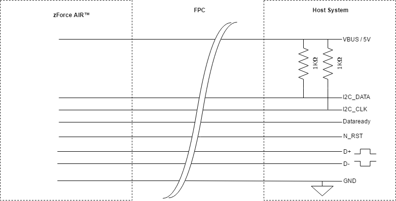
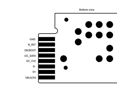
The module can either be configured as an I2C- or an USB HID-device. It has 8 contact pads, compatible with a standard FFC-connector with 1 mm in pitch. The host needs to be connected to all 8 pads even though only I2C or USB HID is used.
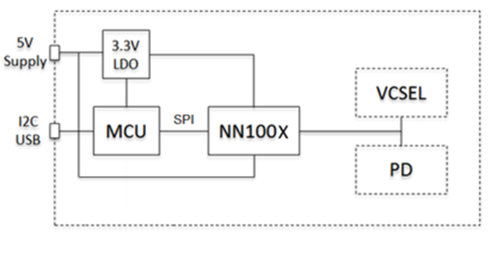
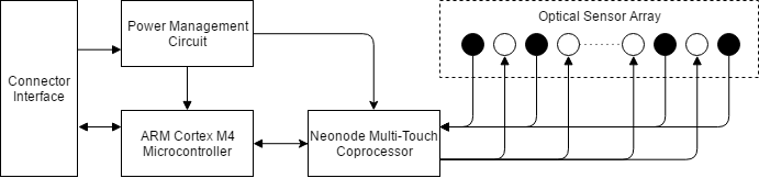
Electrical Block Diagram Module Interface
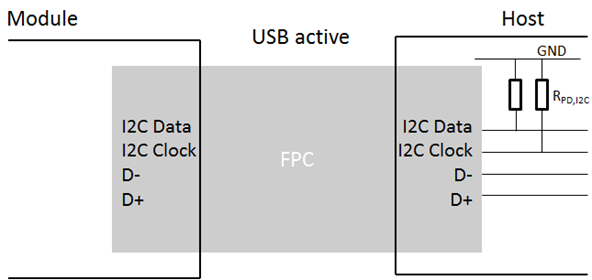
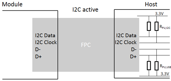
The module supports two standard interfaces, USB and I2C.
Module Pin-Out


Note: All I/O have 3.3V voltage level and are 5V tolerant.
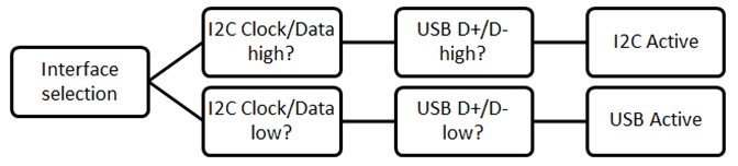
I2C and USB Configuration
The selection for which interface is active can be controlled by proper termination of the unused interface on the host side. The values RPU,I2C depends on the I2C Clock speed (rise/fall times, the bus load and output/input min and max values). For termination of a unused interface, Neonode recommends 1kΩ pullup/pulldown.
When an I2C host is present, the I2C Clock and Data line must be pulled high by pull up resistors (as according to I2C specification).
In the case of USB interface, the host transceiver will have 15kΩ pulldown resistor for both D+/D- line. So D+/D- will always be low before enumeration has started.
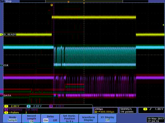
DR PIN Characteristics in I2C Configuration
After the device is powered on, the default state of this DR pin is Low (‘0’). Then, after the FW finishes the initialization, it will waiting to send out a boot complete notification. Then this pin will be set to High (‘1’).
This pin will be set to High (‘1’) when there is data in buffer to be sent from I2C.
This pin will be reset to Low (‘0’) when there is no data in buffer to be sent from I2C.
There is no requirement whether this pin is in interrupt mode or not on the host side. When this pin is set to high, FW will keep waiting for host to read data from I2C bus. When the ‘Read’ transaction happens, FW will clear this DR automatically. Below is an oscilloscope screenshot of the timing on I2C.
Normal Boot
During boot up the following sequence will be performed (before any interface is selected):
Bootloader
The onboard MCU has built-in bootloader functionality. When power is applied to the module, the Boot pin will be sampled and if the applied voltage is above 1.4V it will enter bootloader mode and be ready for firmware update. For details regarding bootloader mode, please refer to the following ST Microelectronics application notes:
AN2606 – Bootloader specification
AN4221 - I2C Protocol
AN3156 – USB Protocol
Document generated by Confluence on Sep 11, 2025 11:01