
Electrostatic Sensitive Device!
To prevent equipment damage, use proper grounding techniques.

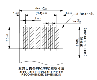
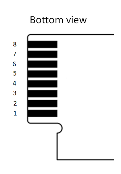
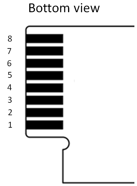
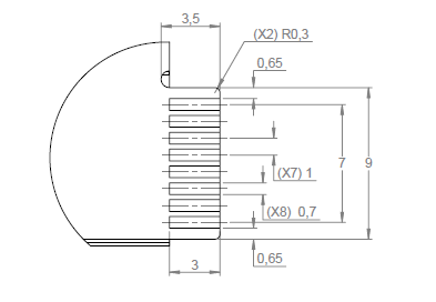
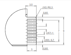
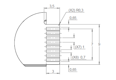
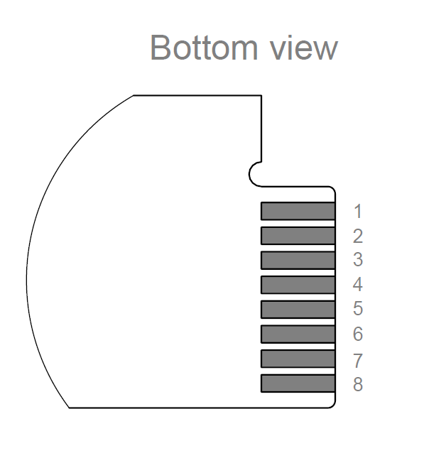
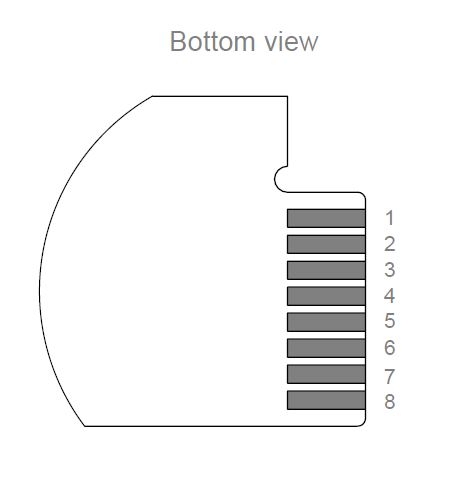
The Touch Sensor has 8 contact pads and a PCB outline that matches that of a standard 0.3-0.33 mm thick FFC/FPC with 1 mm pitch and top mounted connectors:

The contact pads are placed on the backside of the Touch Sensor PCBA.
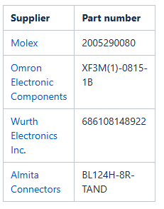
List of supported FFC connectors:

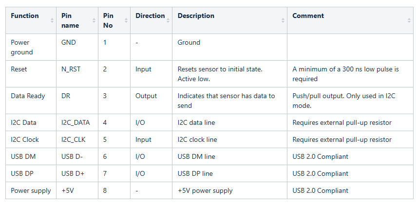
Note: All pins use 3.3V voltage level and have 5V tolerance.
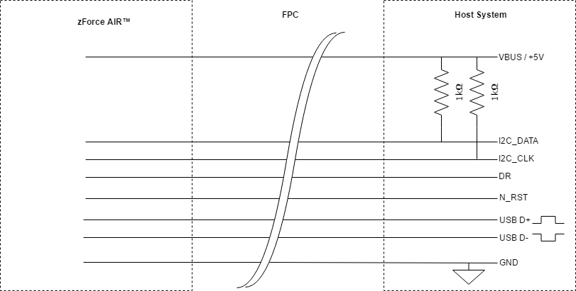
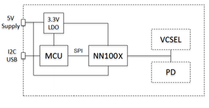
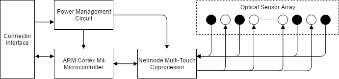
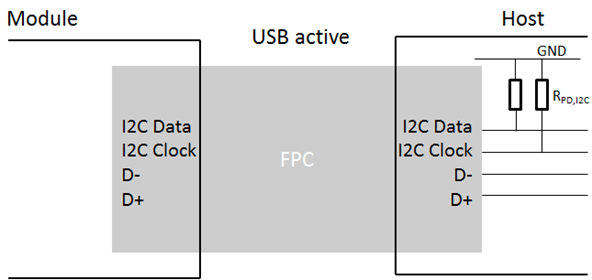
Interface ConfigurationThe zForce AIR Touch Sensor provides two interfaces for communication with the host system, I2C and USB HID-device. The user can choose to connect one of them, or both. The typical Touch Sensor connection to a host system is shown in the following diagram:
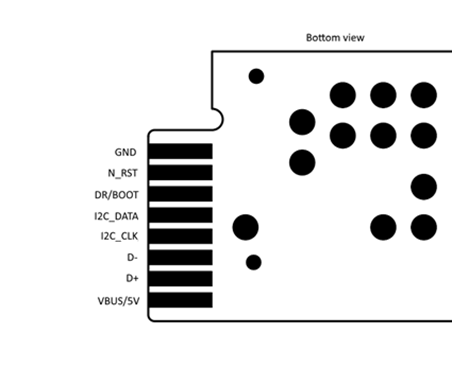
The zForce AIR Touch Sensor provides a USB full-speed device interface through its 8-pin connector. In this connection, PIN 1, 6, 7, 8 ( GND, USB D-, USB D+, VBUS ) are used. After connecting the sensor to the host system, it could be enumerated as a normal USB HID-device and act as a digitizer for a touch screen.
In this connection, only the default touch active area size could be used. Please refer to Product Variants for the actual values.
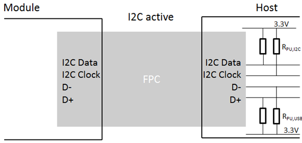
In this case, it is recommended to use two 1k? pull-up resistors to tie up I2C_DATA and I2C_CLK pins to VBUS or 3.3V power supply to avoid noise issue on I2C interface, and leave other pins as not connected. PIN 2 ( N_RST ) could be used to reset or enable/disable the sensor.
USB Characteristics
The USB interface meets the requirements of USB specifictions 2.0:
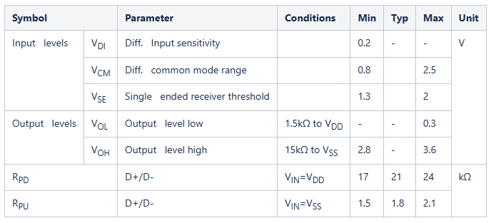
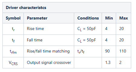
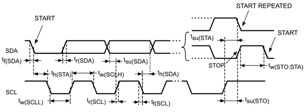
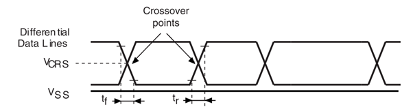
USB full speed timings: the definitions of data signal rise and fall time are presented in the following table and figure:

The zForce AIR Touch Sensor provides an I2C interface through its 8-pin connector. The interface runs in fast mode, which means the speed is 400kbps. With this interface, more advanced configuration could be performed. PIN 1, 3, 4, 5, 8 ( GND, DR, I2C_DATA, I2C_CLK, VBUS ) are used for this connection. It is recommended to use two 1k? pull-up resistors to tie up I2C_DATA and I2C_CLK pins to VBUS or 3.3V power supply to perform proper I2C communication. If USB connection is not used in parallel, PIN 6, 7 ( USB D-, USB D+ ) could be left unconnected.
After the Touch Sensor is powered on, it will act as a slave device on a I2C bus. For further information about what commands could be send or receive through this interface, please refer to I2C Transport.
I2C Characteristics
The I2C interface meets the requirements of the standard I2C communication protocol with the following restrictions: SDA and SCL are mapped to I/O pins that are not “true” open-drain. When configured as open-drain, the PMOS connected between the I/O pin and VDD is disabled, but is still present.
The I2C characteristics are described in the following table:
|
Symbol |
Parameter |
Min |
Max |
Unit |
|---|---|---|---|---|
|
tw(SCLL) |
SCL clock low time |
4.7 |
- |
us |
|
tw(SCLH) |
SCL clock high time |
4.0 |
- |
|
|
tsu(SDA) |
SDA setup time |
250 |
- |
ns |
|
th(SDA) |
SDA data hold time |
0 |
- |
|
|
tr(SDA) |
SDA and SCL rise time |
- |
1000 |
|
|
tr(SCL) |
||||
|
tf(SDA) |
SDA and SCL fall time |
|
300 |
|
|
tf(SCL) |
||||
|
th(STA) |
Start condition hold time |
4.0 |
- |
us |
|
tsu(STA) |
Repeated Start condition setup time |
4.7 |
- |
|
|
tsu(STO) |
Stop condition setup time |
4.0 |
- |
|
|
tw(STO:STA) |
Stop to Start condition time (bus free |
4.7 |
- |
|
|
tSP |
Pulse width of the spikes that are |
0 |
50 |
ns |
|
Cload |
Capacitive load for each bus line |
- |
400 |
pF |
|
V IL |
Input low level voltage |
|
0.8 |
V |
|
V IH |
Input high level voltage |
2.3 |
|
V |
|
V OL |
Output low level voltage |
|
0.4 |
V |
|
V OH |
Output high level voltage |
2.9 |
|
V |

PIN 3 ( DR) Characteristics
PIN 3 is used as signal output for DataReady (DR). The DataReady signal is only used in I2C communication.
The sensor can only act as an I2C slave, therefore this pin is needed to notify the host to read the data in the output buffer of the sensor:
- PIN 3 is set to high (1) when there is data in the buffer to be sent from the sensor.
- PIN 3 is reset to low (0) when there is no data in the buffer to be sent from the sensor.
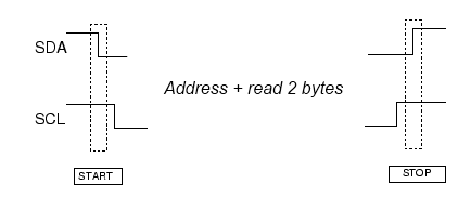
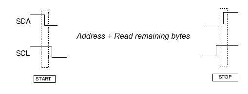
PIN 3 can be used as an interrupt input or it can be read repeatedly by the host. When the pin is set to high, the FW will wait for the host to read data from the I2C bus. When the read transaction is finished, this DataReady signal will be reset automatically by the zForce AIR Touch Sensor. The following figure shows the timing behavior of a typical I2C transaction:
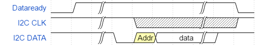
I2C Reading Sequence
See I2C Transport.
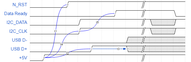
Power On and Boot SequencePower on timing latency are listed in the following table:

The power on sequence is shown in the following figure.

Document generated by Confluence on Sep 11, 2025 11:01